Jan 22, 2025 | Posted by Abdul-Rahman Oladimeji
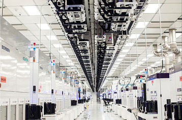
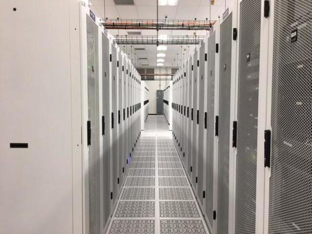
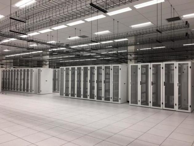
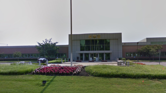
GlobalFoundries (GF) has announced plans to build an Advanced Packaging and Photonics Center in the state of New York, USA, described as the center as “the first of its kind.” The company said the new facility would allow semiconductors to be “securely manufactured, processed, packaged, and tested entirely onshore in the United States.” GF said the AI boom had led to a growing need for silicon photonics and 3D and heterogeneously integrated (HI) chips to meet power, bandwidth, and density requirements in data centers and Edge devices.
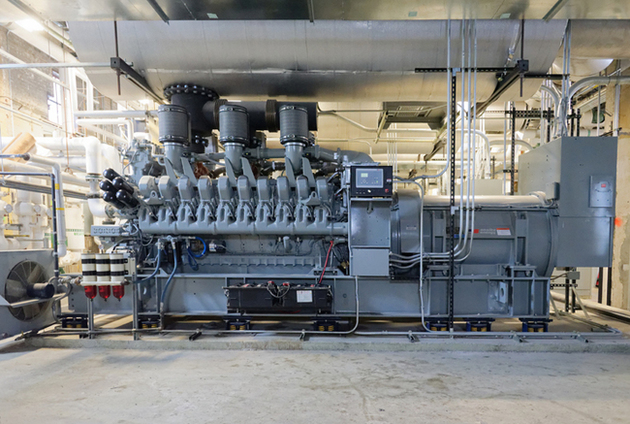
Tthe company said its new Advanced Packaging and Photonics Center will offer advanced packaging, assembly, and testing for GF’s differentiated silicon photonics platform; full turnkey advanced packaging, bump, assembly, and testing for aerospace and defense customers; and new production capabilities for the advanced packaging, wafer-to-wafer bonding, assembly and testing of 3D and HI chips using GF’s 12LP+, 22FDX, and other platforms.
The new center is "a direct response to our customers asking for more geodiversity in their supply chains and additional support with advanced packaging solutions for GF silicon photonics, Trusted, and 3D/HI offerings,” said Dr. Thomas Caulfield, president and CEO of GF. “The New York Advanced Packaging and Photonics Center will be unique in our industry and will play a vital role in the continued growth of the Empire State’s world-class semiconductor manufacturing and innovation ecosystem.”